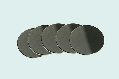
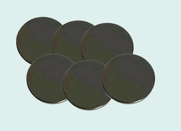
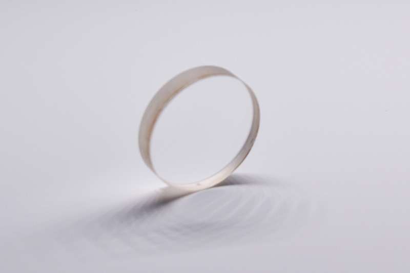
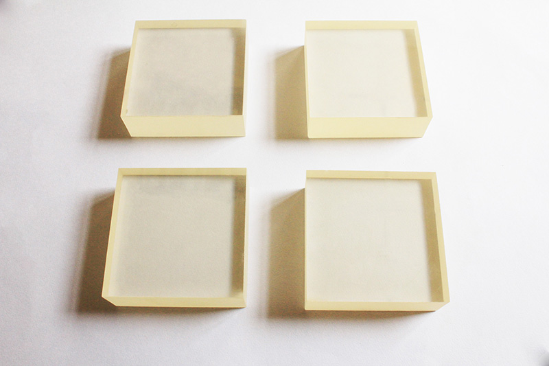
Si Windows
Silicon is a mono crystal primarily used in semi-conductor and is non-absorptive at 1.2μm to 6μm IR regions. It is used here as an optical component for IR region applications.
Silicon is used as an optical window primarily in the 3 to 5 micron band and as a substrate for production of optical filters. Large blocks of Silicon with polished faces are also employed as neutron targets in Physics experiments.
Silicon is grown by Czochralski pulling techniques (CZ) and contains some oxygen which causes an absorption band at 9 microns. To avoid this, Silicon can be prepared by a Float-Zone (FZ) process. Optical Silicon is generally lightly doped ( 5 to 40 ohm cm) for best transmission above 10 microns. Silicon has a further pass band 30 to 100 microns which is effective only in very high resistivity uncompensated material. Doping is usually Boron (p-type) and Phosphorus (n-type).
Application:
• Ideal for 1.2 to 7 μm NIR applications
• Broadband 3 to 12 μm anti-reflection coating
• Ideal for weight sensitive applications
Feature:
• These silicon windows do not transmit at 1µm region or below, therefore its main application is in IR regions.
• Because of its high thermal conductivity, it is suitable for use as a high power laser mirror
▶Silicon windows have a shiny metal surface; it reflects and absorbs but does not transmit in the visible regions.
▶Silicon windows surface reflection results in transmittance loss of 53%. (measured data 1 surface reflection at 27%)
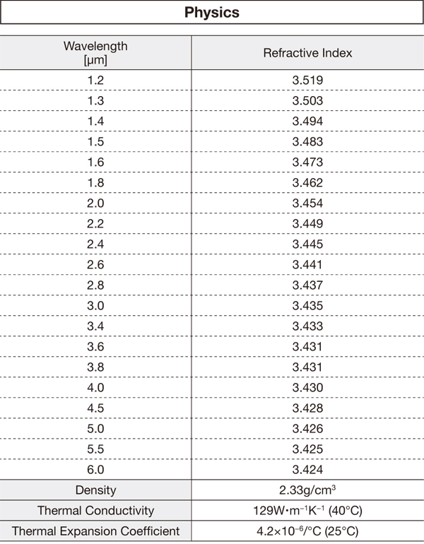
| Transmission Range : | 1.2 to 15 μm (1) |
| Refractive Index : | 3.4223 @ 5 μm (1) (2) |
| Reflection Loss : | 46.2% at 5 μm (2 surfaces) |
| Absorption Coefficient : | 0.01 cm-1 at 3 μm |
| Reststrahlen Peak : | n/a |
| dn/dT : | 160 x 10-6 /°C (3) |
| dn/dμ = 0 : | 10.4 μm |
| Density : | 2.33 g/cc |
| Melting Point : | 1420 °C |
| Thermal Conductivity : | 163.3 W m-1 K-1 at 273 K |
| Thermal Expansion : | 2.6 x 10⁻⁶ / at 20°C |
| Hardness : | Knoop 1150 |
| Specific Heat Capacity : | 703 J Kg-1 K-1 |
| Dielectric Constant : | 13 at 10 GHz |
| Youngs Modulus (E) : | 131 GPa (4) |
| Shear Modulus (G) : | 79.9 GPa (4) |
| Bulk Modulus (K) : | 102 GPa |
| Elastic Coefficients : | C11=167; C12=65; C44=80 (4) |
| Apparent Elastic Limit : | 124.1MPa (18000 psi) |
| Poisson Ratio : | 0.266 (4) |
| Solubility : | Insoluble in Water |
| Molecular Weight : | 28.09 |
| Class/Structure : | Cubic diamond, Fd3m |
Products categories
-

Phone
Phone
-

Email
Email
-

whatsapp
whatsapp
-

Wechat
Wechat

-

Top


